 | ÐлекÑÑоннÑй компоненÑ: CD4053BM | СкаÑаÑÑ:  PDF PDF  ZIP ZIP |
Äîêóìåíòàöèÿ è îïèñàíèÿ www.docs.chipfind.ru
TL F 5662
CD4051BMCD4051BC
CD4052BMCD4052BC
CD4053BMCD4053BC
Analog
MultiplexerDemultiplexers
October 1989
CD4051BM CD4051BC Single 8-Channel Analog
Multiplexer Demultiplexer
CD4052BM CD4052BC Dual 4-Channel Analog
Multiplexer Demultiplexer
CD4053BM CD4053BC Triple 2-Channel Analog
Multiplexer Demultiplexer
General Description
These analog multiplexers demultiplexers are digitally con-
trolled analog switches having low ``ON'' impedance and
very low ``OFF'' leakage currents Control of analog signals
up to 15V
p-p
can be achieved by digital signal amplitudes of
3 15V For example if V
DD
e
5V V
SS
e
0V and V
EE
e b
5V
analog signals from
b
5V to
a
5V can be controlled by digi-
tal inputs of 0 5V The multiplexer circuits dissipate ex-
tremely low quiescent power over the full V
DD
b
V
SS
and
V
DD
b
V
EE
supply voltage ranges independent of the logic
state of the control signals When a logical ``1'' is present at
the inhibit input terminal all channels are ``OFF''
CD4051BM CD4051BC is a single 8-channel multiplexer
having three binary control inputs A B and C and an inhibit
input The three binary signals select 1 of 8 channels to be
turned ``ON'' and connect the input to the output
CD4052BM CD4052BC is a differential 4-channel multiplex-
er having two binary control inputs A and B and an inhibit
input The two binary input signals select 1 or 4 pairs of
channels to be turned on and connect the differential ana-
log inputs to the differential outputs
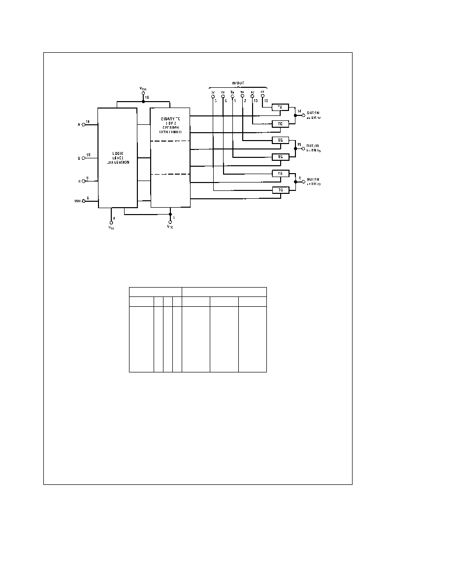
CD4053BM CD4053BC is a triple 2-channel multiplexer
having three separate digital control inputs A B and C and
an inhibit input Each control input selects one of a pair of
channels which are connected in a single-pole double-throw
configuration
Features
Y
Wide range of digital and analog signal levels digital
3 15V analog to 15V
p-p
Y
Low ``ON'' resistance 80X (typ ) over entire 15V
p-p
sig-
nal-input range for V
DD
b
V
EE
e
15V
Y
High ``OFF'' resistance channel leakage of
g
10 pA
(typ ) at V
DD
b
V
EE
e
10V
Y
Logic level conversion for digital addressing signals of
3 15V (V
DD
b
V
SS
e
3 15V) to switch analog signals to
15 V
p-p
(V
DD
b
V
EE
e
15V)
Y
Matched switch characteristics
D
R
ON
e
5X (typ ) for
V
DD
b
V
EE
e
15V
Y
Very low quiescent power dissipation under all digital-
control input and supply conditions
1 mW (typ ) at
V
DD
b
V
SS
e
V
DD
b
V
EE
e
10V
Y
Binary address decoding on chip
Connection Diagrams
Dual-In-Line Packages
CD4051BM CD4051BC
CD4052BM CD4052BC
CD4053BM CD4053BC
TL F 5662 1
Order Number CD4051B CD4052B or CD4053B
C1995 National Semiconductor Corporation
RRD-B30M105 Printed in U S A
Absolute Maximum Ratings
If Military Aerospace specified devices are required
please contact the National Semiconductor Sales
Office Distributors for availability and specifications
DC Supply Voltage (V
DD
)
b
0 5 V
DC
to
a
18 V
DC
Input Voltage (V
IN
)
b
0 5 V
DC
to V
DD
a
0 5 V
DC
Storage Temperature Range (T
S
)
b
65 C to
a
150 C
Power Dissipation (P
D
)
Dual-In-Line
700 mW
Small Outline
500 mW
Lead Temp (T
L
) (soldering 10 sec )
260 C
Recommended Operating
Conditions
DC Supply Voltage (V
DD
)
a
5 V
DC
to
a
15 V
DC
Input Voltage (V
IN
)
0V to V
DD
V
DC
Operating Temperature Range (T
A
)
4051BM 4052BM 4053BM
b
55 C to
a
125 C
4051BC 4052BC 4053BC
b
40 C to
a
85 C
DC Electrical Characteristics
(Note 2)
Symbol
Parameter
Conditions
b
55 C
a
25
a
125 C
Units
Min
Max
Min
Typ
Max
Min
Max
I
DD
Quiescent Device Current
V
DD
e
5V
5
5
150
m
A
V
DD
e
10V
10
10
300
m
A
V
DD
e
15V
20
20
600
m
A
Signal Inputs (V
IS
) and Outputs (V
OS
)
R
ON
``ON'' Resistance (Peak
R
L
e
10 kX
V
DD
e
2 5V
for V
EE
s
V
IS
s
V
DD
)
(any channel
V
EE
e b
2 5V
800
270
1050
1300
X
selected)
or V
DD
e
5V
V
EE
e
0V
V
DD
e
5V
V
EE
e b
5V
310
120
400
550
X
or V
DD
e
10V
V
EE
e
0V
V
DD
e
7 5V
V
EE
e b
7 5V
200
80
240
320
X
or V
DD
e
15V
V
EE
e
0V
D
R
ON
D
``ON'' Resistance
R
L
e
10 kX
V
DD
e
2 5V
Between Any Two
(any channel
V
EE
e b
2 5V
10
X
Channels
selected)
or V
DD
e
5V
V
EE
e
0V
V
DD
e
5V
V
EE
e b
5V
10
X
or V
DD
e
10V
V
EE
e
0V
V
DD
e
7 5V
V
EE
e b
7 5V
5
X
or V
DD
e
15V
V
EE
e
0V
``OFF'' Channel Leakage
V
DD
e
7 5V
V
EE
e b
7 5V
Current any channel
O I
e
g
7 5V I O
e
0V
g
50
g
0 01
g
50
g
500
nA
``OFF''
``OFF'' Channel Leakage
Inhibit
e
7 5V
CD4051
g
200
g
0 08
g
200
g
2000
nA
Current all channels
V
DD
e
7 5V
``OFF'' (Common
V
EE
e b
7 5V
CD4052
g
200
g
0 04
g
200
g
2000
nA
OUT IN)
O I
e
0V
I O
e
g
7 5V
CD4053
g
200
g
0 02
g
200
g
2000
nA
Control Inputs A B C and Inhibit
V
IL
Low Level Input Voltage
V
EE
e
V
SS
R
L
e
1 kX to V
SS
I
IS
k
2 mA on all OFF channels
V
IS
e
V
DD
thru 1 kX
V
DD
e
5V
1 5
1 5
1 5
V
V
DD
e
10V
3 0
3 0
3 0
V
V
DD
e
15V
4 0
4 0
4 0
V
V
IH
High Level Input Voltage
V
DD
e
5
3 5
3 5
3 5
V
V
DD
e
10
7
7
7
V
V
DD
e
15
11
11
11
V
Note 1
``Absolute Maximum Ratings'' are those values beyond which the safety of the device cannot be guaranteed Except for ``Operating Temperature Range''
they are not meant to imply that the devices should be operated at these limits The table of ``Electrical Characteristics'' provides conditions for actual device
operation
Note 2
All voltages measured with respect to V
SS
unless otherwise specified
2
DC Electrical Characteristics
(Note 2) (Continued)
Symbol
Parameter
Conditions
b
40 C
a
25 C
a
85 C
Units
Min
Max
Min
Typ
Max
Min
Max
I
IN
Input Current
V
DD
e
15V
V
EE
e
0V
b
0 1
b
10
b
5
b
0 1
b
1 0
m
A
V
IN
e
0V
V
DD
e
15V
V
EE
e
0V
0 1
10
b
5
0 1
1 0
m
A
V
IN
e
15V
I
DD
Quiescent Device Current
V
DD
e
5V
20
20
150
m
A
V
DD
e
10V
40
40
300
m
A
V
DD
e
15V
80
80
600
m
A
Signal Inputs (V
IS
) and Outputs (V
OS
)
R
ON
``ON'' Resistance (Peak
R
L
e
10 kX
V
DD
e
2 5V
for V
EE
s
V
IS
s
V
DD
)
(any channel
V
EE
e b
2 5V
850
270
1050
1200
X
selected)
or V
DD
e
5V
V
EE
e
0V
V
DD
e
5V
V
EE
e b
5V
330
120
400
520
X
or V
DD
e
10V
V
EE
e
0V
V
DD
e
7 5V
V
EE
e b
7 5V
210
80
240
300
X
or V
DD
e
15V
V
EE
e
0V
D
R
ON
D
``ON'' Resistance
R
L
e
10 kX
V
DD
e
2 5V
Between Any Two
(any channel
V
EE
e b
2 5V
10
X
Channels
selected)
or V
DD
e
5V
V
EE
e
0V
V
DD
e
5V
V
EE
e b
5V
10
X
or V
DD
e
10V
V
EE
e
0V
V
DD
e
7 5V
V
EE
e b
7 5V
5
X
or V
DD
e
15V
V
EE
e
0V
``OFF'' Channel Leakage
V
DD
e
7 5V
V
EE
e b
7 5V
Current any channel ``OFF'' O I
e
g
7 5V I O
e
0V
g
50
g
0 01
g
50
g
500
nA
``OFF'' Channel Leakage
Inhibit
e
7 5V
CD4051
g
200
g
0 08
g
200
g
2000
nA
Current all channels
V
DD
e
7 5V
``OFF'' (Common
V
EE
e b
7 5V
CD4052
g
200
g
0 04
g
200
g
2000
nA
OUT IN)
O I
e
0V
I O
e
g
7 5V
CD4053
g
200
g
0 02
g
200
g
2000
nA
Control Inputs A B C and Inhibit
V
IL
Low Level Input Voltage
V
EE
e
V
SS
R
L
e
1 kX to V
SS
I
IS
k
2 mA on all OFF Channels
V
IS
e
V
DD
thru 1 kX
V
DD
e
5V
1 5
1 5
1 5
V
V
DD
e
10V
3 0
3 0
3 0
V
V
DD
e
15V
4 0
4 0
4 0
V
V
IH
High Level Input Voltage
V
DD
e
5
3 5
3 5
3 5
V
V
DD
e
10
7
7
7
V
V
DD
e
15
11
11
11
V
I
IN
Input Current
V
DD
e
15V
V
EE
e
0V
b
0 1
b
10
b
5
b
0 1
b
1 0
m
A
V
IN
e
0V
V
DD
e
15V
V
EE
e
0V
0 1
10
b
5
0 1
1 0
m
A
V
IN
e
15V
Note 1
``Absolute Maximum Ratings'' are those values beyond which the safety of the device cannot be guaranteed Except for ``Operating Temperature Range''
they are not meant to imply that the devices should be operated at these limits The table of ``Electrical Characteristics'' provides conditions for actual device
operation
Note 2
All voltages measured with respect to V
SS
unless otherwise specified
3
AC Electrical Characteristics
T
A
e
25 C t
r
e
t
f
e
20 ns unless otherwise specified
Symbol
Parameter
Conditions
V
DD
Min
Typ
Max
Units
t
PZH
Propagation Delay Time from
V
EE
e
V
SS
e
0V
5V
600
1200
ns
t
PZL
Inhibit to Signal Output
R
L
e
1 kX
10V
225
450
ns
(channel turning on)
C
L
e
50 pF
15V
160
320
ns
t
PHZ
Propagation Delay Time from
V
EE
e
V
SS
e
0V
5V
210
420
ns
t
PLZ
Inhibit to Signal Output
R
L
e
1 kX
10V
100
200
ns
(channel turning off)
C
L
e
50 pF
15V
75
150
ns
C
IN
Input Capacitance
Control input
5
7 5
pF
Signal Input (IN OUT)
10
15
pF
C
OUT
Output Capacitance
(common OUT IN)
CD4051
10V
30
pF
CD4052
V
EE
e
V
SS
e
0V
10V
15
pF
CD4053
10V
8
pF
C
IOS
Feedthrough Capacitance
0 2
pF
C
PD
Power Dissipation Capacitance
CD4051
110
pF
CD4052
140
pF
CD4053
70
pF
Signal Inputs (V
IS
) and Outputs (V
OS
)
Sine Wave Response
R
L
e
10 kX
(Distortion)
f
IS
e
1 kHz
10V
0 04
%
V
IS
e
5 V
p-p
V
EE
e
V
SI
e
0V
Frequency Response Channel
R
L
e
1 kX V
EE
e
0V V
IS
e
5V
p-p
10V
40
MHz
``ON'' (Sine Wave Input)
20 log
10
V
OS
V
IS
e b
3 dB
Feedthrough Channel ``OFF''
R
L
e
1 kX V
EE
e
V
SS
e
0V V
IS
e
5V
p-p
10V
10
MHz
20 log
10
V
OS
V
IS
e b
40 dB
Crosstalk Between Any Two
R
L
e
1 kX V
EE
e
V
SS
e
0V V
IS
(A)
e
5V
p-p
10V
3
MHz
Channels (frequency at 40 dB)
20 log
10
V
OS
(B) V
IS
(A)
e b
40 dB (Note 3)
t
PHL
Propagation Delay Signal
V
EE
e
V
SS
e
0V
5V
25
55
ns
t
PLH
Input to Signal Output
C
L
e
50 pF
10V
15
35
ns
15V
10
25
ns
Control Inputs A B C and Inhibit
Control Input to Signal
V
EE
e
V
SS
e
0V R
L
e
10 kX at both ends
Crosstalk
of channel
10V
65
mV (peak)
Input Square Wave Amplitude
e
10V
t
PHL
Propagation Delay Time from
V
EE
e
V
SS
e
0V
5V
500
1000
ns
t
PLH
Address to Signal Output
C
L
e
50 pF
10V
180
360
ns
(channels ``ON'' or ``OFF'')
15V
120
240
ns
AC Parameters are guaranteed by DC correlated testing
Note 3
A B are two arbitrary channels with A turned ``ON'' and B ``OFF''
4
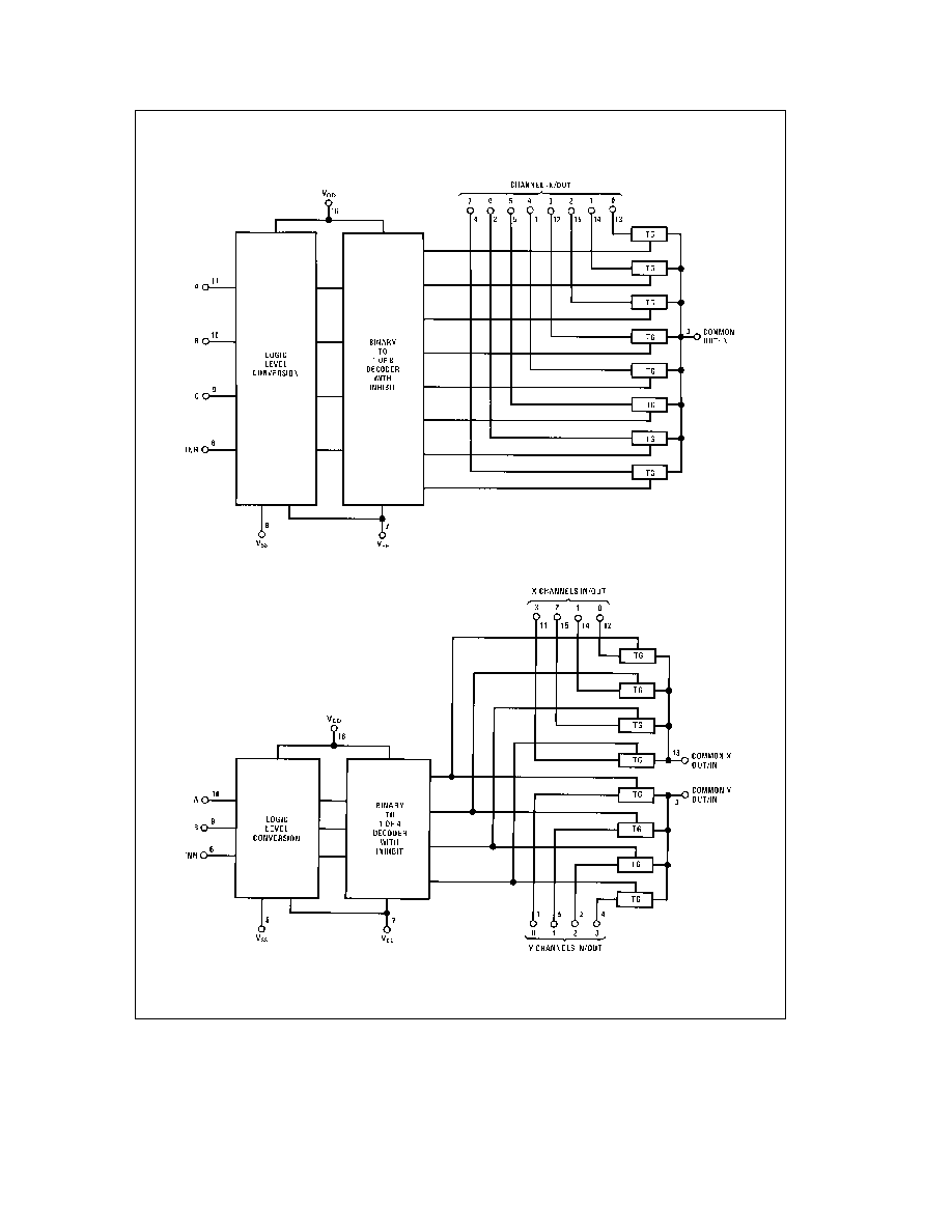
Block Diagrams
CD4051BM CD4051BC
CD4052BM CD4052BC
TL F 5662 2
5
Block Diagrams
(Continued)
CD4053BM CD4053BC
TL F 5662 3
Truth Table
INPUT STATES
``ON'' CHANNELS
INHIBIT
C
B
A
CD4051B
CD4052B
CD4053B
0
0
0
0
0
0X 0Y
cx bx ax
0
0
0
1
1
1X 1Y
cx bx ay
0
0
1
0
2
2X 2Y
cx by ax
0
0
1
1
3
3X 3Y
cx by ay
0
1
0
0
4
cy bx ax
0
1
0
1
5
cy bx ay
0
1
1
0
6
cy by ax
0
1
1
1
7
cy by ay
1
NONE
NONE
NONE
Don't Care condition
6
Switching Time Waveforms
TL F 5662 4
7
Special Considerations
In certain applications the external load-resistor current may
include both V
DD
and signal-line components To avoid
drawing V
DD
current when switch current flows into IN OUT
pin the voltage drop across the bidirectional switch must
not exceed 0 6V at T
A
s
25 C or 0 4V at T
A
l
25 C (calcu-
lated from R
ON
values shown) No V
DD
current will flow
through R
L
if the switch current flows into OUT IN pin
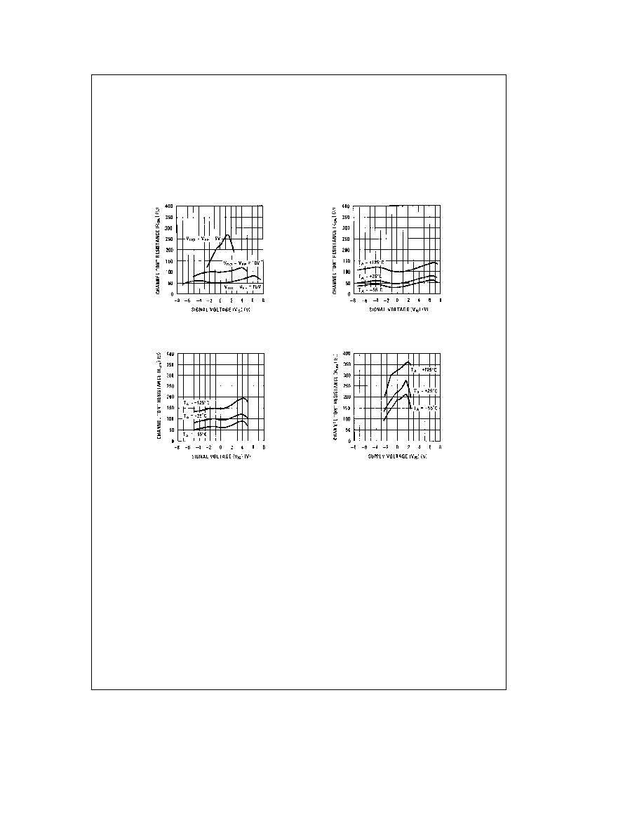
Typical Performance Characteristics
``ON'' Resistance vs Signal
Voltage for T
A
e
25 C
``ON'' Resistance as a
Function of Temperature for
V
DD
b
V
EE
e
10V
``ON'' Resistance as a
Function of Temperature for
V
DD
b
V
EE
e
15V
``ON'' Resistance as a
Function of Temperature for
V
DD
b
V
EE
e
5V
TL F 5662 5
8
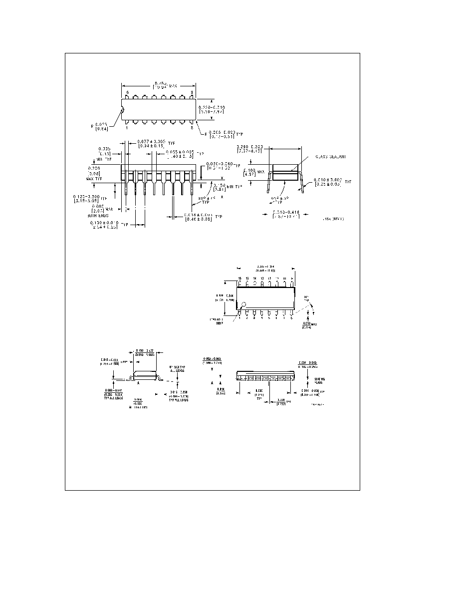
Physical Dimensions
inches (millimeters)
Cavity Dual-In-Line Package (J)
Order Number CD4051BMJ CD4051BCJ CD4052BMJ
CD4052BCJ CD4053BMJ or CD4053BCJ
NS Package Number J16A
Small Outline Package (M)
Order Number CD4051BCM
CD4052BCM or CD4053BCM
NS Package Number M16A
9
CD4051BMCD4051BC
CD4052BMCD4052BC
CD4053BMCD4053BC
Analog
MultiplexerDemultiplexers
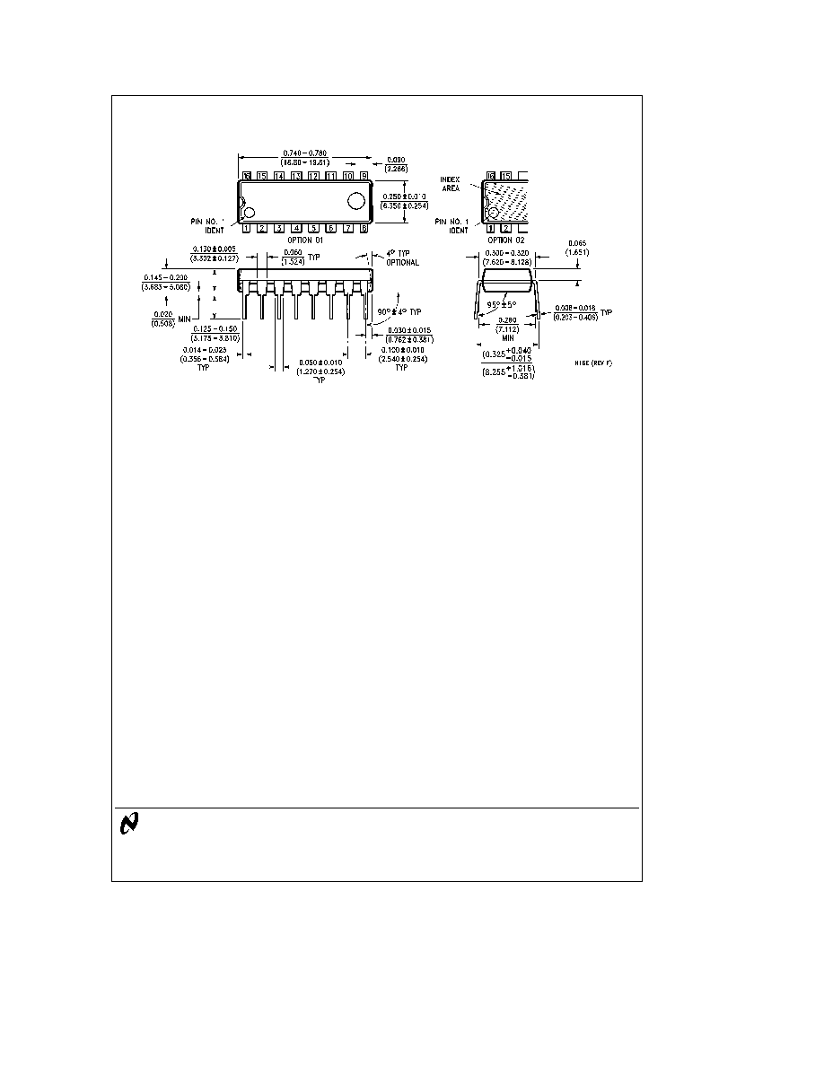
Physical Dimensions
inches (millimeters) (Continued)
Molded Dual-In-Line Package (N)
Order CD4051BM CD4051BC
CD4052BM CD4052BC CD4053BM CD4053BC
NS Package Number N16E
LIFE SUPPORT POLICY
NATIONAL'S PRODUCTS ARE NOT AUTHORIZED FOR USE AS CRITICAL COMPONENTS IN LIFE SUPPORT
DEVICES OR SYSTEMS WITHOUT THE EXPRESS WRITTEN APPROVAL OF THE PRESIDENT OF NATIONAL
SEMICONDUCTOR CORPORATION As used herein
1 Life support devices or systems are devices or
2 A critical component is any component of a life
systems which (a) are intended for surgical implant
support device or system whose failure to perform can
into the body or (b) support or sustain life and whose
be reasonably expected to cause the failure of the life
failure to perform when properly used in accordance
support device or system or to affect its safety or
with instructions for use provided in the labeling can
effectiveness
be reasonably expected to result in a significant injury
to the user
National Semiconductor
National Semiconductor
National Semiconductor
National Semiconductor
Corporation
Europe
Hong Kong Ltd
Japan Ltd
1111 West Bardin Road
Fax (a49) 0-180-530 85 86
13th Floor Straight Block
Tel 81-043-299-2309
Arlington TX 76017
Email cnjwge tevm2 nsc com
Ocean Centre 5 Canton Rd
Fax 81-043-299-2408
Tel 1(800) 272-9959
Deutsch Tel (a49) 0-180-530 85 85
Tsimshatsui Kowloon
Fax 1(800) 737-7018
English
Tel (a49) 0-180-532 78 32
Hong Kong
Fran ais Tel (a49) 0-180-532 93 58
Tel (852) 2737-1600
Italiano
Tel (a49) 0-180-534 16 80
Fax (852) 2736-9960
National does not assume any responsibility for use of any circuitry described no circuit patent licenses are implied and National reserves the right at any time without notice to change said circuitry and specifications